We are strategic Partner for Energy grid, AI, Semiconductors, MCU Design, Digital Twins, Holography and IoT Projects 

With our experience your solution will achieve not only makeup but will enable next gen of your products!
Strategy to roll out of your product to WW market, 20+ years of experience with award wining products portfolio.

We are - cofounder of Czech National Semiconductor Cluster, initiator of Czech National Semiconductor Strategy, Czech Competence Center. Active participants on Pilar I of EU Chips Act, aCCCess, EuroCDP, ENCCC.

In order to turn your vision to reality with the most experienced business development with detailed technical expertise, contact us!


LOCATION

Brno , Czech Republic 60200

E-MAIL

cerny@smarterinstruments.eu

PHONE +420 602548732

LinkedIn

https://www.linkedin.com/in/stanislav-cerny-27746a27/


Our Services

Business development 

After pioneering of first CZ IPCEI ME/CT establishment success as official elected National ICP we offer

- guidance thru whole IPCEI process, matchmaking, project portfolio, konsortium agreement, etc

Guidance is different from agencies, because of real technical expertise and large experience from the EU and national implementation 

Partnership for project to provide high valued embedded systems and AI references and skills. 40 years in semiconductor business

Holographic Solutions & Transportation

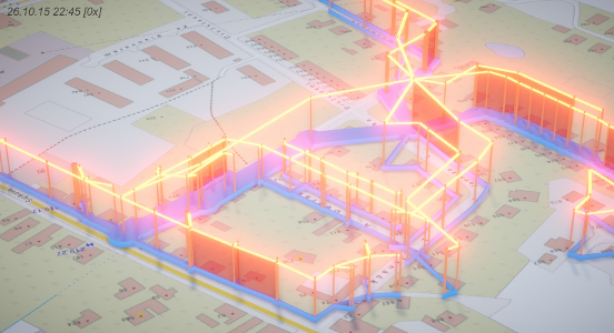
Lightfield technologies allow our customers three dimensional naked eye experience with their objects, datas, holographic images and videos.

Our excellent visual engineering team with deep experience of lightfield technologies, GPU processing, image acquisition works on the latest technologies such as lightfield displays and holographic acquistion systems  in order to develop the top visual quality applications for your product portfolio.

We could create value added solution for your market and also deliver components, like holographic displays and acquisition rigs to meet your needs for applications.

Regarding long time experience with SW tools WW development and delivery in semiconductor industry,  integration with your tools and our holographic technology is in professional hands.

Three dimensional interactive scene, controlled in real time by naked hands and observed by naked hands is standard solution of our company. Also it's delivery to any place of the world.

Strategic partnership with chipmakers

20 years of experience in semiconductor industry, cooperation with most of semiconductor vendors, embedded systems HW & SW design, relation with universities, European Commission awarded products - consistent background you can count with for your solutions. We will always choose the most suitable solution for your IoTproject. 

01

Smarter Metering

We are looking forward, smart is not enough, our solutions are much smarter thru innovation in HMI, advanced backup solutions, extended nodes lifecycle. 

Our solutions for smart metering bring true innovation and added value for both distribution network and end user. Extended lifecycle and danced power solutions don't need dangerous elements such as replaceable batteries for communication modules, thus maintenance cost are dropped significantly for thousands of nodes. Modular architecture of our interfaces allow use pin compatible communication modules from Telit and always meet demands of the customers for desired communication.

LTE -M supported : NB1, CAT M1, 3G backward compatibility is possible according to requirements. Modules used are certified to work over globe.

Latest projects

02

IPCEI ME/CT

Key role as National Industry Contact

Project SLAID - Ultra low power Edge AI for low performance MCUs ARM Cortex M33 plus with capability to adapt as key feature for the mass IoT devices deployment. 

IPCEI AST - submission in process 

ICP help for Crytur, onsemi, MycroftMind, SVCS, Valeo and others participant.


Lets Chat

LOCATION

Lidicka 28, Brno, Czech Republic 60200


E-MAIL

cerny@smarterinstruments.eu

PHONE

+420 602 548 732

FOLLOW US


© Copyright SmarterInstruments